Compound semiconductors create analytical challenges
Our everyday lives are changing at a rapid pace. The evolution of transportation, renewable energy, and communication has led to surging demand for higher performance power electronics. As a result, we have seen significant acceleration in the development of power device designs, most notably the transition to wide bandgap (WBG) compound semiconductors that overcome the operating voltage and frequency limitations of silicon-based devices.
Incorporating compound semiconductors brings about its own set of challenges, mainly due to the increased defects inherent in these materials. Reducing critical dimensions and transitioning to vertical designs raise the potential for failures, such as gate oxide breakdown and threshold voltage instability caused by charge trapping, exacerbated during high-voltage operation.
With failures on the rise, precise localization and subsequent preparation and analysis of the root cause mechanism are critical to improve device reliability and performance and to realize the promise of wide bandgap semiconductors. This article explores the pivotal role of focused ion beam scanning electron microscopy (FIB SEM) and transmission electron microscopy (TEM) in the evolving landscape of advanced power device failure analysis.
New FIB SEM capabilities
Physical failure analysis of semiconductor devices with FIB SEM is a widely adopted technique, owing to precise material removal and high-resolution imaging of structures below the surface. However, traditional Ga+ FIB preparation does not yield optimal results in wide bandgap semiconductor materials with different chemical and physical properties.
SiC is harder and more resistant to Ga+ FIB milling than the surrounding metals and oxides in a MOSFET device. This makes it difficult to avoid differential milling artifacts in a SEM cross-section or TEM lamella, unless low currents are used, which increases the time needed for preparation. However, the advanced FIB design of the Thermo Scientific Helios 5 Hydra DualBeam provides a unique advantage, using selectable ion plasma species to significantly improve both milling quality and throughput. When using the Ar+ source, the Helios 5 Hydra DualBeam can generate a polished surface with fewer curtains in half the time compared to Xe+ (Figure 1) and 20 times faster than Ga+.
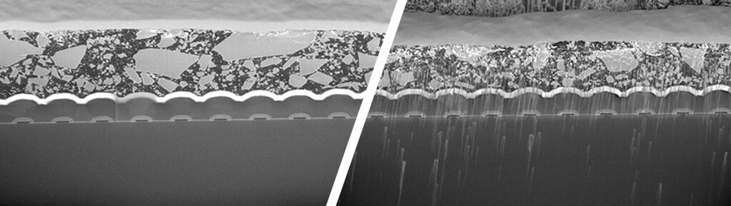
Figure 1: SiC MOSFET cross-sections prepared using the Helios 5 Hydra DualBeam Ar+ (left) and Xe+ FIB (right).
Ensuring uniformity and accuracy of critical dimensions throughout the device is crucial for its performance. For a more comprehensive analysis, 3D-reconstruction of Ar+ FIB tomography data reveals the complete internal structure with enhanced segmentation through elemental analysis and mapping (Figure 2). Thermo Scientific Avizo 3D Software automatically reports key measurements, helping you to quickly understand relevant trends and to make decisions.
 HEMT 3D reconstruction showing wide bandgap layers.")
Figure 2: Gallium nitride (GaN) HEMT 3D reconstruction with segmented device layers.
Ar+ FIB lamella preparation also increases TEM data quality compared to Xe+, and even low-energy Ga+ (Figure 3), by minimizing amorphous damage. When a thicker amorphized layer is present, the atomic lattice structure is obscured and materials within the region of interest are more difficult to resolve, limiting measurement and mapping precision.

Figure 3: TEM images comparing Si lattice resolution of lamella prepared by Ar+, Xe+, and Ga+ FIB.
Transmission electron microscopy “ground truth” analysis of wide bandgap materials
Scanning transmission electron microscopy is an incredibly powerful tool, often providing the root cause “ground truth” answers in most failure analysis workflows. Scanning transmission electron microscopy systems such as the Thermo Scientific Talos F200E (S)TEM and Spectra 200 (S)TEM provide insights into critical areas, including crystalline defects, metrology, and composition. Determining epitaxial layer properties, strain and diffusion mapping, and p/n junction visualization, are examples of the many analyses enabled by scanning transmission electron microscopy. Coupling energy dispersive X-ray spectroscopy (EDS) (Figure 4) and electron energy-loss spectroscopy (EELS) with atomic-resolution imaging facilitates comprehensive understanding of the material composition and properties using simultaneous heavy and light element detection with chemical bonding information.

Figure 4: The Talos F200E (S)TEM enables “time-resolved”/zero-damage Super-X EDS analysis of a GaN HEMT device.
More than ever, it is critical to stay at the forefront of analytical capabilities in the ever-evolving field of semiconductor technology. As shown by real examples of failure analysis techniques in advanced power semiconductor devices, new FIB SEM and scanning transmission electron microscopy techniques play a pivotal role in identifying failure mechanisms and guiding improvements in device design. With the insights from the Helios 5 Hydra Dualbeam and the Talos F200E TEM, device reliability and performance goals can be achieved with wide bandgap semiconductor materials, enabling continued success and growth in the booming market of electrical power management and control.
Click here to learn more about wide bandgap semiconductor device failure analysis

Physical and Electrical Failure Analysis of Power Semiconductor Devices
World energy consumption is expected to grow by nearly 50% b...
Read More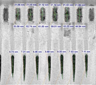
Revolutionizing the way TEM metrology data is collected
As I discussed in my 2024 year-end article, the semiconducto...
Read More
Leave a Reply