Preparing semiconductor samples for failure analysis and metrology
As logic, memory, display and power semiconductors advance, performing failure analysis and metrology has become more difficult because of high-ratio 3D structures, packaged die, novel materials and more complex circuit density. With each advancement, the availability of statistically relevant data with sub-nanometer scale accuracy is critical for identifying defects and out of tolerance process steps. Increasingly, obtaining high-quality data starts with a high-quality sample.
With today’s semiconductors, preparing a high-quality sample is not always an easy task. A high-quality sample devoid of damage and artifacts is required whether you need to:
- Quickly remove large volumes of materials to find a nanometer-scale defect in a large area;
- Remove small volumes of materials to perform site-specific analysis; or
- Prepare a lamella for transmission electron microscopy (TEM) analysis.
While each of these applications have similarities, they also have unique challenges that can result in a lower quality sample.
In this blog series, we’ll discuss the sample preparation challenges associated with each of these applications and the characteristics needed in focused ion beam scanning electron microscopes (FIB-SEM).
- Blog two: Nanoscale Microscopy with Gallium FIB-SEM
- Blog three: Why TEM Lamella Preparation Dictates Data Quality
This first post highlights high-speed large volume material removal, some of challenges encountered, and provides recommendations on key characteristics to look for in a FIB-SEM, such as the Thermo Scientific Helios 5 Plasma FIB, the Thermo Scientific Helios 5 Laser PFIB and the Thermo Scientific Helios 5 Hydra to address these challenges.
Large-volume material removal for large area analysis and imaging
Within the semiconductor industry, there is a need for high-speed, large volume material removal with precise site-specific analysis and imaging capabilities. This is particularly useful when you need to remove hundreds of micrometers (µm) to millimeters (mm) of material to perform physical failure analysis or remove thick layers to access a region of interest (ROI) over a large area. While the goal may be to remove the large volumes of material quickly, it is important that the FIB-SEM provides precise and accurate cut placements to avoid obfuscation of nanometer scale defects, and that is does not damage the sample.

Thick copper (Cu) removal performed with a Thermo Scientific Helios 5 PFIB
Removing large volumes of materials across a large area can create challenges for delivering high-quality samples. In the next sections, we’ll discuss three challenges; curtaining effects, damage to the sample and preparation of samples containing dissimilar materials and recommend capabilities to look for in a FIB-SEM to address these challenges.
Curtain propagation and large-volume material removal
A challenge that may occur with an interaction involving the beam and a non-homogeneous specimen, such as milling or cross-sectioning, is curtaining. Curtaining can occur when milling through a sample or structure containing different materials with variable milling rates. This interaction results in a variation or unevenness in topography of the milled face that looks like scratches or striations that, in some cases, make detailed analysis difficult or impossible in some cases. To address the potential issues caused by curtaining, sample preparation operators should look for instruments that support capabilities such as rocking polish.
With curtaining, it should be noted it can negatively impact both small-volume and large volume sample preparation. However, with large-volume material removal, curtaining can propagate rapidly with dissimilar materials and large cross-sections.
When there is a need to perform uniform large-area planar milling, a technique that can be very valuable is spin mill. For those not familiar with spin mill, the technique removes a thin layer from the sample surface at a nearly glancing angle. During the milling process, the stage is periodically rotated to a series of pre-defined milling sites. This efficiently removes material over a large planar area to provide a smooth surface for imaging, nanoprobing or additional cross-sectioning work.
These capabilities: cross-sectioning and spin mill, are available with the Thermo Scientific Helios 5 PFIB and the Thermo Scientific Helios 5 Laser PFIB.
Sample damage and lasers
When there is a need to quickly remove a large volume of material over a large area for cross-sectioning, nothing compares to a laser. Where a PFIB enables material removal at a rate of approximately 106 µm3/hr., a laser can remove approximately 10 mm3/hr. However, it should be noted, while many laser types exist, some have more desirable milling characteristics than others.
For example, while “nanosecond” lasers can effectively remove material by ablation (spot/targeted vaporization of a defined area), it may result in unwanted, extreme damage to the area surrounding the ROI. Microcracking may form in a large heat-affected zone due to thermal stresses, shock waves, and the melting and cooling of the surrounding material.

Lucas, L. and J. Zhang, Femtosecond laser micromachining: a back-to-basics primer. 2012, http://www.industrial-lasers.com/
In contrast, femtosecond (fs) lasers can propagate energy in short fs pulses with greater instantaneous intensity. This quickly accelerates local ablation, so that the ablated material does not have time to transfer thermal energy to the surrounding material and most of the absorbed energy is used to gasify the solid phase into a plasma.

The heat impact of a long pulse versus a short pulse laser. Reference: Randolph, Steven & Filevich, Jorge & Botman, Aurelien et al. (2018). In situ femtosecond pulse laser ablation for large volume 3D analysis in scanning electron microscope systems. Journal of Vacuum Science & Technology B. 36. 06JB01. 10.1116/1.5047806.
Solutions that utilize a femtosecond laser, and ideally one that is integrated into a single chamber, such as the Thermo Scientific Helios 5 Laser PFIB are recommended. Integrating the laser into single chamber eliminates navigation misalignments and the potential for sample contamination when moving the sample. These issues can frequently occur with solutions that utilize two chambers or an ex-situ laser.
Preparing samples with dissimilar materials
Preparing samples with multiple types of stacked material is becoming increasingly common. Using a 2.5D and 3D package to illustrate. These structures consist of several hierarchal packaging levels with a single die or a stack of multiple dies. With the integration of multiple dies, the result can be a package containing several disparate materials with some soft and some hard like silicon carbide (SiC). This can make producing a high-quality sample a unique challenge. Stacked materials with different sputter rates can cause extreme curtaining and introduce unwanted thermal behaviors, both of which can result in an inability to properly analyze and cause damage to the sample.
When dealing with dissimilar materials, two factors that can have a positive impact on the ability to remove a large volume of material and produce high-quality samples are, ion species and the angle of incidence of the beam to the sample.
Any interaction between the beam and the specimen, such as milling or cross-sectioning, will result in sputtering and curtaining. In an ideal world, the ion beam would evenly remove all types of material without artifacts. As this is not possible, one way to reduce the sputtering across disparate materials such tungsten and silicon is to optimize the beam’s incident angle as the beam’s angle can impact the sputter rate. Of course, as you go deeper into the device, the incidence angle of the beam will get steeper.
-

- A monocrystalline silicon sample prepared with xenon (Xe+). The Xe+ took 1 minute, 42 seconds at 2.5µA.
-

- A monocrystalline silicon sample prepared with argon (Ar+). The Ar+ took 58 seconds at 3.7µA. Both uses of Xe+ and Ar+ demonstrate the excellent beam profile of the Thermo Scientific Helios 5 Hydra.
The second factor to consider is the angle of incidence. We know that certain ion species can mill more uniformly than others for different substrate types. For example, xenon (Xe) and argon (Ar) are non-interactive ion species which make them ideal for cross-sectioning. In comparison, oxygen which interacts both chemically and physically during the milling process, is extremely effective for milling through hard materials such as silicon carbide (SiC), diamond and other carbon containing materials. In addition to having the capability to utilize different ion beam species, it is also essential capability to be able to switch from one to another in a matter of minutes.
For those that are regularly working on samples containing multiple material types, the flexibility of Thermo Fisher Scientific Helios 5 Hydra is invaluable for sample preparation and subsequent analysis.
Conclusions
Today’s sample preparation must span a wide variety of applications. When performing large volume material removal; curtaining, sample damage and lasers, and preparing samples with dissimilar materials may be encountered and Thermo Fisher’s FIB-SEM solutions can help mitigate these challenges.
Our next blog post will highlight the challenges faced when preparing site specific samples and the important methodology behind doing so accurately.
The Thermo Scientific Helios 5 Family
The Thermo Scientific Helios 5 PFIB, Helios 5 Laser PFIB and Helios 5 Hydra are part of the Helios 5 family, which includes the broadest selection of FIB-SEMs to meet the semiconductor industry’s sample preparation needs. Below are the FIB-SEMs mentioned in this blog.
-

- Helios 5 PFIB DualBeam
-

- Helios 5 Laser PFIB
-

- Helios 5 Hydra DualBeam

//
David Akerson is a Senior Marketing Manager at Thermo Fisher Scientific

Transmission Electron Microscopy in Semiconductors: Generating Ground Truth Insights
What is the current state of TEM in semiconductor analysis? ...
Read More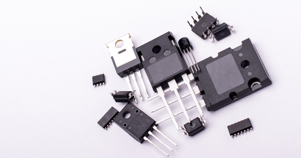
Physical and Electrical Failure Analysis of Power Semiconductor Devices
World energy consumption is expected to grow by nearly 50% b...
Read More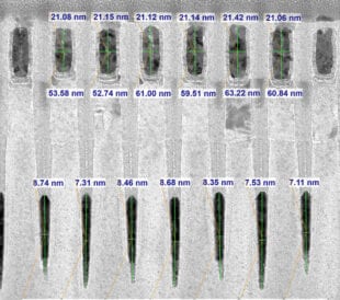
Revolutionizing the way TEM metrology data is collected
As I discussed in my 2024 year-end article, the semiconducto...
Read More
Leave a Reply