World energy consumption is expected to grow by nearly 50% between 2018 and 2050. As much of our power shifts over to electricity, higher-efficiency, compact power semiconductor devices, such as diodes, IGBTs, MOSFETs and HEMTs are needed to run everything from smart phones and electric vehicles to industrial robots.
Today, the semiconductor industry is moving beyond silicon to develop the next generation of power devices. Wide bandgap power devices make it possible to build higher performance, more reliable components that improve power efficiency and operate at higher temperatures. Unfortunately, these materials can introduce new failure modes—and using traditional electrical failure analysis to identify root cause can be challenging, potentially impacting operational reliability and manufacturing yields.
Take silicon metal-oxide semiconductor field-effect transistors (MOSFETs), for example. These transistors, designed to handle high power requirements, are the workhorse for a majority of switching power applications. Yet as higher voltages and frequencies are packaged into ever smaller form factors, the performance of these power MOSFETs is reaching its limit.
By redesigning power MOSFETs using new semiconductor materials such as silicon carbide and gallium nitride, engineers can develop cost-effective solutions for power switching that meet the needs for highly efficient and compact power semiconductor devices.
The limits of traditional electrical failure analysis methods
As engineers design these devices, the main challenge is eliminating circuit shorts. Unlike integrated circuits made up of billions of tiny transistors connected by layers of thin wires, power devices are composed of one transistor with one thin wire that’s completely covered by a single sheet of metal. This design makes it difficult to isolate and characterize small leakage paths—and requires different electrical failure analysis methodologies than were used in the past.
Emission microscopy and optical beam induced resistivity change (OBIRCH) are the traditional methods for pinpointing power MOSFET failure modes. Yet these methods are hampered by the thick sheet of metal covering the surface. To overcome this limitation, engineers sometimes use reactive ions or wet chemicals to open windows into the metal to better access the failure. The downside of this method is reproducibility is low and the likelihood of completely disabling the device is high.

New methods are needed as engineers work to design state-of-the-art power devices that include wide bandgap materials
A robust workflow for next-generation power semiconductor devices
To address these issues, Thermo Fisher Scientific developed a robust workflow that combines electrical failure analysis (EFA) to isolate faults and physical failure analysis (PFA) to characterize the microstructure—helping engineers to pinpoint anomalous electrical behavior at the microstructural level. Not only is this workflow faster and more accurate, but it generates repeatable results with little to no destruction of the device.
Read our latest application note: Transforming failure analysis of wide bandgap power MOS devices >>
The workflow involves the following steps:
Electrical failure analysis of power semiconductor devices
- Localizing the region of interest: The Thermo Scientific ELITE System is used to coarsely isolate the fault by detecting heat emitted anywhere on the device, regardless of the presence of the sheet of metal covering the surface. What makes ELITE unique is the ability to lock in the detector to a ramped bias and acquire separate amplitude and phase signals. Amplitude is the same signal as a basic thermal microscope, and it generally provides a misleading failure location. The ELITE’s phase signal overcomes this problem with its increased sensitivity to the source of the heat, rather than where the heat accumulates.
- Opening a window through the metal sheet: The Thermo Scientific Helios 5 PFIB DualBeam uses a fine beam of inert gas ions to open a window in the metal sheet at the location indicated by the ELITE. A gas is flowed over the sample to produce a uniformly flat-bottomed opening over the device. The electron microscope in the DualBeam is used to stop the ion milling process precisely at an appropriate layer within the device. In some cases, the “delayering” stops when the metal sheet is removed, and the source contacts are just exposed. In other cases, the device is delayered further into the gate electrode. Under this sample preparation protocol, the power semiconductor device remains fully functional, with the behavior of the original part unchanged.
- Nanoprobing to further localize the defect: If the defect isn’t exposed during the PFIB delayering step, nanoprobing is applied to further localize the fault. Scanning electron microscope (SEM) nanoprobing using the Thermo Scientific nProber IV System, or atomic-force probing using the Thermo Scientific Hyperion System positions fine probes in discrete locations of the region of interest to extract current-voltage curves. Anomalies in the current-voltage curve reveal the location of the fault and indicate the volume of material that must be examined to find the defect using physical fault analysis.
Physical failure analysis of power semiconductor devices
- Characterizing the microstructure responsible for the failure: The Helios 5 PFIB DualBeam is used to prepare the sample using two possible approaches:
- Slice and view: This technique involves making a series of FIB cuts followed by SEM imaging as cuts are made through the material until the defect is found. If more detailed imaging is required to characterize the defect, a thin sample can be prepared and imaged using a scanning transmission electron microscope (STEM) such as the Thermo Scientific Talos Transmission Electron Microscope (TEM).
- Direct to the Talos TEM: The alternative sample prep approach is to extract a piece of the material up to a few microns thick using the Helios PFIB DualBeam and move the sample directly into the Talos TEM. This is the fastest approach, but thicker samples may require additional thinning and analysis to conclusively characterize the defect.

Dopant revealed in a Silicon Carbide IGBT
As engineers design state-of-the-art power management solutions, they need new failure analysis methods that help them to precisely isolate and characterize faults. Thermo Fisher’s EFA to PFA workflow offers a fast and accurate way to improve power device quality—paving the way for the next generation of power devices needed to power our global economy.

//
Roger Alvis is a lead product specialist at Thermo Fisher Scientific.
High-Quality TEM Lamella Preparation: Critical Factors and Best Practices
Introduction: The quality of transmission electron microscop...
Read More
Removing Large Volumes of Material Fast with FIB-SEMs
Focused ion beam scanning electron microscopes (FIB-SEMs) ar...
Read More
Transmission Electron Microscopy in Semiconductors: Generating Ground Truth Insights
What is the current state of TEM in semiconductor analysis? ...
Read More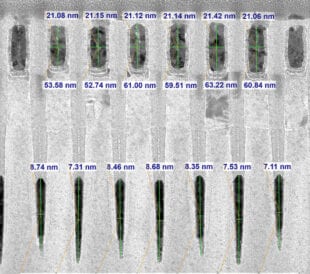
Revolutionizing the way TEM metrology data is collected
As I discussed in my 2024 year-end article, the semiconducto...
Read More
Leave a Reply