It’s an exciting time for cutting edge semiconductor technology advancement. Semiconductor researchers are experimenting with new materials and compounds, aggressively exploring novel, complex 3D structures to deliver future generations of logic, memory, display and power devices. As semiconductor development efforts explore the boundaries of physics and the physical properties of materials, gaining structural and chemical insights becomes ever more challenging. Higher precision, atomic-level engineering and reproduceable workflows become paramount, and require a new generation of scanning transmission electron microscopy.
Optimizing data acquisition with scanning transmission electron microscopy
Scanning transmission electron microscopy requires extremely accurate, site specific samples. Yet getting these high-value, delicate samples to the lab, and capturing quality data from them, is challenging.
For example, the latest gate-all-around technology contains multiple stacked channels that may be of the order of 20nm in length. The extremely precise characterization processes around these channels must be accurately managed to ensure optimal and repeatable electrical performance. The complex structure may also contain new materials whose behavior under an electron beam may be unknown or worse, be susceptible to damage at high voltages.
Engineering samples are often costly and in short supply, so it is important to maintain the sample’s integrity to capture as much data as possible. The following methods are critical to guaranteeing the integrity of samples every time:
- Tailor the electron beam parameters to the sample in question. Ensure the dose (beam current) and applied voltage are adjusted to get the required scanning transmission electron microscopy data while maintaining sample integrity.
- Capture complete data in real time to allow the operator to “turn back time” to a point before the applied beam has any effect on the sample. This guarantees data is collected from every sample.
- Invest in the fastest, most efficient detection system to enable data capture as quickly as possible with the lowest dose.
Only the best for atomic-scale semiconductor research
While it is true that most leading-edge scanning transmission electron microscopy systems have the capability to perform atomic-scale analysis, newer generation systems can provide a comprehensive set of solutions for current and emerging challenges.
For example, the latest instruments now have Energy Dispersive Spectroscopy (EDS) detectors that are three to six times faster than those available five years ago.
This means that elemental data can be extracted from a sample more quickly, saving time and preventing unnecessary, and potentially damaging, interactions between the beam and highly sensitive samples.
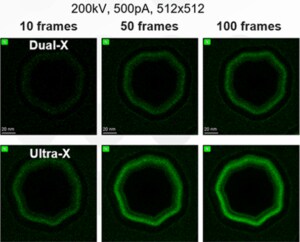
3D NAND sample nitrogen maps at 10, 50 and 100 frames
Fast accelerating voltage switching
Most transmission electron microscopes tend to be used at one operating voltage, typically at 200kV. Switching between operating voltages was time consuming and frequently resulted in many hours of waiting for the required stabilization. The breadth of today’s applications further challenges these constraints. For example:
- High accelerating voltages are typically optimal for high resolution imaging and thick samples, such as through focus imaging or EELS analysis.
- Lower (<100kV) accelerating voltages are optimal for performing EDS analysis, or for imaging fragile samples that may suffer knock-on damage.
This puts those in semiconductor research in a situation where, if their sample type or application varied from one day to the next, they were forced to work with just one operating voltage, often resulting in sub-optimal data collection.
Fortunately, scanning transmission electron microscopy solutions are evolving to support researchers as semiconductor advancements become more challenging.
One of our latest semiconductor advancements, the Thermo Scientific Spectra Ultra, provides fast switching of the operating voltage, enabling researchers to control the beam parameters to perform experiments requiring high resolution or analysis on beam sensitive samples within minutes. This provides unprecedented experimentation capabilities and time savings while sidestepping the sacrifices previous generations required.

HAADF and EDS maps from an AlGaAs/GaAs interface taken at 300 kV and 200 kV in less than one hour. Reducing the accelerating voltage reduces specimen damage (compare e and f) and improves the EDS signal (compare c and d). Specimen courtesy of J. Zweck, University of Regensburg
Scanning transmission electron microscopy operating software is also evolving.
Over the past 30 years, operating software has advanced from simple scripting languages to highly productive, menu-driven interfaces, which include features such as time-resolved imaging. This increases the probability that you will get the best results from each individual sample.
This is an exciting period of innovation in both semiconductor technology and electron microscopy, and Spectra Ultra is breaking the constraints that have restricted advanced semiconductor research, enabling a new era of atomic-scale device engineering.

Learn more about the Spectra Ultra >>

Transmission Electron Microscopy in Semiconductors: Generating Ground Truth Insights
What is the current state of TEM in semiconductor analysis? ...
Read More
Physical and Electrical Failure Analysis of Power Semiconductor Devices
World energy consumption is expected to grow by nearly 50% b...
Read More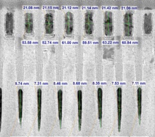
Revolutionizing the way TEM metrology data is collected
As I discussed in my 2024 year-end article, the semiconducto...
Read More
Leave a Reply